Issue 1, January 1984 - Spectrum Keyboard Buffer
| Home | Contents | KwikPik |
| Issue 3 | "Some Speccys 'ave Adam" |
|
Most people who want to modify and improve their Spectrum look first
at the keyboard as a prime area for change. But straightforward
replacement involves digging around inside the computer - something
of a put-off, for two important reasons.
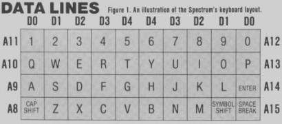
To begin with it might nullify the guarantee from Sinclair and, frankly, there's just no-one else around to undertake this kind of repair work (there's no published circuit diagram and a lack of certain specialised parts). Secondly, it's easy for damage to occur when fitting the keyboard to the computer or mounting the keyboard in a separate case (which requires the removal of the complete circuit board from the casing of the computer). So what's outlined here is a keyboard buffer that fits on the back of the ZX Spectrum, connecting to the real expansion port. It can easily be fitted or unplugged for testing, and should your Spectrum develop a fault, it can be removed without trace for guarantee purposes. KEYBOARD: FUNCTION & DESIGNThe Sinclair keyboard, like many others, works on a matrix of keys where each key connects up two wires. The combination of the incoming and outgoing wires is continually being tested by the computer to see which one has been pressed. On the ZX Spectrum the keyboard has eight incoming wires - the upper eight address lines. These are tested by holding only one of them to a Binary 0 (a LOW signal) and seeing what the result is on the incoming (data) lines. If a switch has been pressed on the address line being tested, then the LOW signal will be passed on to the data line to which it is connected. Until then the data line will be held to a Binary 1 by the resistors connected to the five data lines.In the keyboard layout diagram (Figure 1) the keys as you can see are arranged in a similar order to the keyboard (but not in the familiar QWERTY layout). The five data line connections are shown at the top and the address lines at the sides. There is only one address line and one data line combination that can be produced by each key. The 'A' key, for instance, will operate only when the A9 address line is tested |
and will pass on the signal to the D0 data line if pressed.
The 'scanning' of the keyboard (as it is called) is done by use of an IN A(C) instruction in machine code which lowers the address lines in turn, starting with A8 and progressing to A15, checking for a keypress on the data lines as it does so. It uses the B and C registers inside the Z-80A to give the 16-bit address (which is put out on the address lines A0 to A15). This is done every 1/50th of a second using the timer within the ULA to trigger an INTERRUPT instruction to the Z-80A microprocessor. The keyboard port is referred to as FE in hexadecimal notation or 254 in decimal, but operates as long as the A0 address line is a LOW signal (Binary 1). The electronics for the port is located within the ULA, and the data lines must be connected through the ULA to the microprocessor only when the correct address is detected. Connecting them straight to the data lines of the Z-80A would cause utter confusion as both the address and data lines are used for other devices as well, like the RAM. DECODING THE KEYBOARD PORTThe keyboard buffer's port must operate in the same way as that of the ZX Spectrum in order to work properly - but with modifications such that the keyboard connected to the buffer will override the internal keyboard.The ULA only uses three lines to tell it when the keyboard port should operate and we shall do the same. The IORQ line determines that it is an IN or an OUT instruction, the RD line that it is a READ instruction into the Z-80A and the A0 address line that it is the correct address. Only when all of these are Binary 1 (LOW) is the address correct, and the data lines from the keyboard connected to the Z-80A. As these are all correct when they are LOW, we can use a device called a NOR gate to detect this. On our three input NOR gates (part of the 74LS27) only when all three inputs are LOW will the output change to Binary 1 (HIGH). See the circuit diagram (Figure 2). As the buffer chips we are using (the 74LS245s) operate on a LOW signal we need to change this HIGH signal from the first gate into a LOW signal. | |
|
D I Y SPECTRUM KEYBOARD BUFFER | ||
| Frigging with the rigging is not as difficult as you might at first think. Stephen Adams gives comprehensive instructions on linking the Spectrum to an alternative keyboard, via its rear expansion port. | ||
| ||
|
We use the second NOR gate in the chip to do this. As all the inputs
to the second gate are HIGH when the address is correct and all LOW at
any other time (the NOR gate always reverts to a LOW output) the
output will be LOW when the address is correct.
This LOW signal is used to operate a buffer which just appears to be transparent to the data lines when the OE line (pin 19) is LOW. When it is HIGH the outputs are disconnected and have no effect on the microprocessor. This is called a high impedance or tristate buffer as it can present three conditions, high impedance (disconnected in simplicity), Binary 1 or Binary 0 (from the inputs). If nothing is connected to the inputs (ie. no switch has been pressed) the internal resistors of the chip set the inputs (and thus the outputs if the OE line is LOW) to Binary 1, just like the Sinclair keyboard). The data lines from the 74LS245 are connected to the data lines via 1.5K ohm resistors to enable you to use the existing keyboard as well as the new one. This is an option that can be cancelled by installing wire straps instead of resistors. These were left in as a further development of this board is to use it to connect up Atari type joysticks to the Sinclair and people may still want to use the buffer board only for the joysticks. The other 74LS245 chip is permanently operated in its WRITE mode (ie. towards the IC socket) by connecting pin 1 to the +5 volt line. The OE pin is also connected to the 0 volt line making its outputs always available. Thus any changes on the upper eight address lines appear on the pins 1 to 8 of the IC socket. The data line buffer chip is always in its READ mode by connecting it to the 0 volt line. The keyboard is not being described as the user can build their own from keyswitches bought as part of a kit (such as those from Maplin or Ambit) or purchased on their own. Alternatively, a keyboard can be bought from many ZX suppliers both with and without a case to plug into the keyboard sockets. In this case you can plug it into the IC socket when it has been modified. MODIFYING THE IC SOCKETIt's very difficult (if not impossible) to buy a socket of the type used on the Sinclair Research computers. This consists of an eight and a five holed in-line socket which uses metal flaps to trap the very thin, metal covered, mylar strips that make up the keyboard connections.A particular type of IC socket, however, uses a similar arrangement to hold in the IC. This is called the Zetronics socket and a 16-pin type is required. They are blue in colour and the two, white metal strips can be clearly seen on both sides of the pin holder. They can be obtained from Maplin, Ambit and others. |
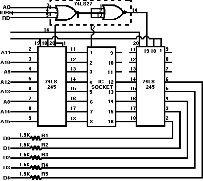
Figure 2. The circuit diagram of the Spectrum's keyboard buffer. | |
The only modification that needs to be done is to use a sharp
craft-type knife to cut away the plastic separations between each of
the IC pin holders. This you do by slicing the socket on the top along
the gap between the two metal strips on each side of the holder that
makes up the pin holders. Once this is cleared away the strip can be
pushed all the way into the socket, the data lines at the top and the
address lines at the bottom. The address lines are the wider of the
two strips.
CONSTRUCTING THE BOARDThe first step is to insert the ICs and the edge connector temporarily into the board to give an idea of where the straps go. These should not be soldered in at this time. The veroboard design has been numbered and lettered to make it easy to identify the holes (see Figure 3).Only one awkward strap exists which is the one connecting A0 to the 74LS27 IC pin 3. This must be taken through the hole in the 'legs' of the edge connector below where the keyway is. All of the ICs go the same way round (including the IC socket) with the cutout or dot on the left-hand side. Thus pin 1 should always be the first pin on the bottom left-hand side and the last pin (14, 16 or 20) on the top left-hand side. Great care has been taken to check the straps shown, the bare wires are indicated by single lines and the insulated straps by fatter ones. The strap from AF9 to AF12 goes over, but does not touch, the strap below it (which goes from AA10 to AG10). The strap from B1 to E1 does the same. All straps should be inserted before |
the ICs are soldered in and the
tracks on the opposite side of the board should be cut only after the
straps have been done. This means that any mistakes can be checked
for, before any irreversible cutting has taken place.
Once the straps and resistors (if required) have been put in, the ICs can be inserted and soldered. The edge connector should be fitted last and should have small sleeves inserted over the last leg at each end to hold it 0.3 inches away from the veroboard. These can be made out of small pieces of insulation stripped from the straps. This is to allow room between the board and the case of the ZX Spectrum which is left untouched. A printed circuit board edge can be fitted at the back, soldered to the pins of the edge connector. This would need to be 28 strips of 0.1 inch spaced board with a keyway cut at pin 5. These can be purchased from Haven Hardware, Timedata and other ZX hardware suppliers. The edge connectors can be obtained from your author. TESTINGBefore the board is connected to the ZX Spectrum, check that there is no direct connection between the +5 volt line and the 0 volt line. These, and all the other connections to the ZX Spectrum, can be found on page 180 of the Basic programming manual. For some unknown reason the top connections are at the bottom and the bottom connections at the top. The only way to check these connections is to turn the book upside down, then you'll get the image of the connections at the back of the computer! The IOROGE should not be used instead of the IORQ. | |
|
The board should be connected to the computer with the power off, the
power then being turned on by plugging-in the jack plug at the back of
the computer. The plug should be immediately removed if the screen
does not show the copyright message after clearing the screen. If this
does happen then try connecting up a data line and an address line on
the IC socket(it can do no harm). This should simulate a keypress and
the screen should show the key pressed. If held on for more than a
second it should repeat. Neither of the SHIFT keys will do this, so
try another key.
If this did not happen, then check all the connections again - if you get coloured squares on the screen it could be that the data IC is permanently operated, so check the connections to pin 19 and the 74LS27. Also check that the address or data lines are not accidentally connected together. Complete failure of any picture would seem to suggest a power fault of some kind, so check the +5 volt and 0 volt lines. If you get the Sinclair Research copyright sign, but none of the combinations work, try using the keyboard. If you have not put the resistors in, but used straps instead, then this should be inoperative, showing that the data buffer IC is being operated correctly. Then check the address lines. A temporary solution when checking address lines that do not work is to solder a piece of wire on to one of the data lines (to the IC socket) and touch that directly on to the edge connector (for that address line). This should operate the key. Once the connections to the IC socket have been checked and operate as they should, the keyboard can be connected. If you are building your own it might be worth investing in a "16-pin DIL header" to make the connections to the IC socket (in which case the modifications to the IC socket are unnecessary).
|
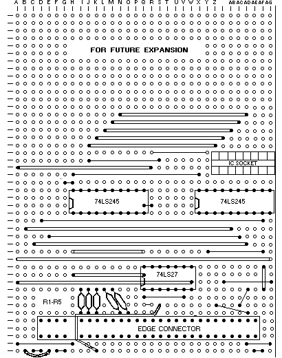
Figure 3. The top illustration shows the component side of the veroboard. The strip side of the keyboard buffer is shown below. The veroboard has been numbered and lettered to help you identify where the components go. 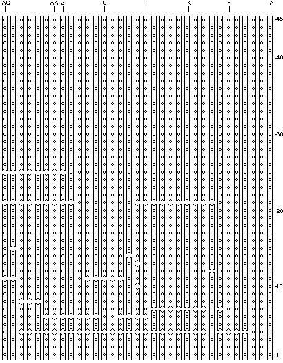
|
| Home | Contents | KwikPik |